The Next Exponential: Computing for Everyone
Kepler is taking on the physical limits of computing to unlock intelligence abundance.
Our two-act plan replaces memory first and then logic with revolutionary material-science and device breakthroughs. We restore Moore’s law economics for fabs by lowering the node transition cost and risks with technology complementary to the maturing EUV-CMOS technology.
Imagine a world where every child, woman, and man can draw on abundant computing power. What could such a planet create—the music, the stories, the scientific breakthroughs? What untapped markets and transformative inventions remain trapped behind today’s walls of affordability and access?
Now imagine the opportunity lost if we fail to act on it.
This is why we built Kepler.
The barriers to an abundance of intelligence are rooted in physics. We are overcoming them by confronting the hardest problems in devices, materials, heat flow, packaging and interconnects.
The limits of today’s AI deployment stem directly from the end of Moore’s Law. For the past 6 decades, computer chips have improved in cost and energy efficiency exponentially following the famous virtuous law - Moore’s Law. The exponential adoption of computing was balanced by the exponential improvements in cost and energy. One negative exponent in time (energy, cost per device) cancelled the other positive exponent (number of devices). As the cost scaling of Moore’s law failed, that same accelerating adoption created an exponential demand for capital. As energy scaling failed, it created an exponential demand for grid scale power.
Today’s logic scaling depends increasingly on two formidable tools: EUV lithography and relentless optimization of logic-cell layouts (FinFLEX1). They preserve density scaling—but at the price of unprecedented equipment sophistication, design complexity, and fab capital intensity. The technical part of Moore's law continues only in equivalent density scaling but not in voltage, energy or SRAM scaling. The Complementary Metal Oxide Semiconductor (CMOS) transistor, has reached its fundamental limits (outlined beautifully by Bob Colwell2 (architect’s perspective) and Dr. Kelin Kuhn3 (device perspective). SRAM scaling has slowed sharply in virtually all axes namely voltage scaling and frequency scaling with cell density peaking near 50 Mb/mm2 .
HBM Memory emerged as the primary scaling driver for AI throughput (TOPS) and energy efficiency (TOPS/W). Even with the industry’s impressive HBM roadmap, we must note that the HBM energy is dominated by the interconnects which are ultimately driven at a voltage required to overcome the Vt limitations of the CMOS transistor4. The HBM economics are dominated by the high ratio of DRAM wafers/HBM (~3 as reported in Hotchips 2026) and the package complexity. While HBM has an exceptional scaling trajectory, the gap with the memory capacity and bandwidth demands of LLMs is extremely high5 and growing.
Developing the next generation of transistors and hence memories and logic requires substantial time, investment and risk6. The result is a rapidly shrinking landscape of foundries, memory makers, concentrating the means to produce new chips in abundance. Leading edge compute (chip) manufacturing is more concentrated and constrained than at any time since the dawn of the computing era.
These are precisely the times when a technical breakthrough can reset the technology.
The Kepler Way: Hard Science for Hard Engineering
Our approach is to recover improvements in energy per operation, memory capacity and useful functions per footprint through physical innovation.
The limits of today’s CMOS are not the fundamental limits of digital computing. There is enormous physical headroom (>1000X) between present-day devices and the minimum energy associated with manipulating digital information7. Our long-term goal is to turn that headroom into thousandfold gains through successive advances in materials, devices and systems.
Our search starts with a simple question: can a material hold information reliably while using very little energy to switch? We compare switching energy Esw with the stability energy E(±Θ) of its information-bearing states8:
Our team has spent more than fifteen years9, across earlier research and at Kepler, looking for materials, memories and devices. A search which spanned a plethora of channel materials, TFETs and their derivatives, spintronics and alternate forms of computing which can beat CMOS in density and energy but preserve the computer architectures. Beyond this ratio (λ) a useful device must hold a reliable state and change it when commanded. Turning a promising material into a memory or logic circuit also requires speed, dynamic and static variation control, reliability, manufacturability and integration with the rest of the system. While the direction was clear as early as 20187, the exact methods were a missing puzzle. So we went after it !
Going beyond the 3D approaches in Act 1, Kepler is building the SRAM replacement memory that scales beyond transistor limits and allows fully customizable DRAM class density in a logic fab.
The materials which have superior λ (~2) lend directly to be SRAM replacements. They are non-volatile due to high stability but they have high switching efficiency. We have worked hard to perfect the reliability and speed of these devices and integrated them into logic fabs.
Kepler is discovering the next switch that beats CMOS, fixes interconnect power and logic scaling.
While AI computation is widely understood to be limited by memory energy, the dominant share of the HBM energy is expended in the dense interconnects (40-100 nm wide) inside and to the memory10, whose energy needs are set by the transistors. It turns out the interconnect capacitance/length is a fundamental constant (πє/ln(AR), where є is the dielectric permittivity and AR the aspect ratio of the wire. The memory access energy which is dominated by interconnect energy is therefore
Hence, the interconnect energy/length scaling requires a reduction in the voltage. There is no free lunch or easy way out to solve the interconnect problems at that scale. We can use packaging to reduce the length to an extent but the energy consumption ultimately needs lower voltages which means a new transistor or a gain element that functions at <300 mV, ideally 100 mV or lower. This is why we are compelled to find a new gain element.
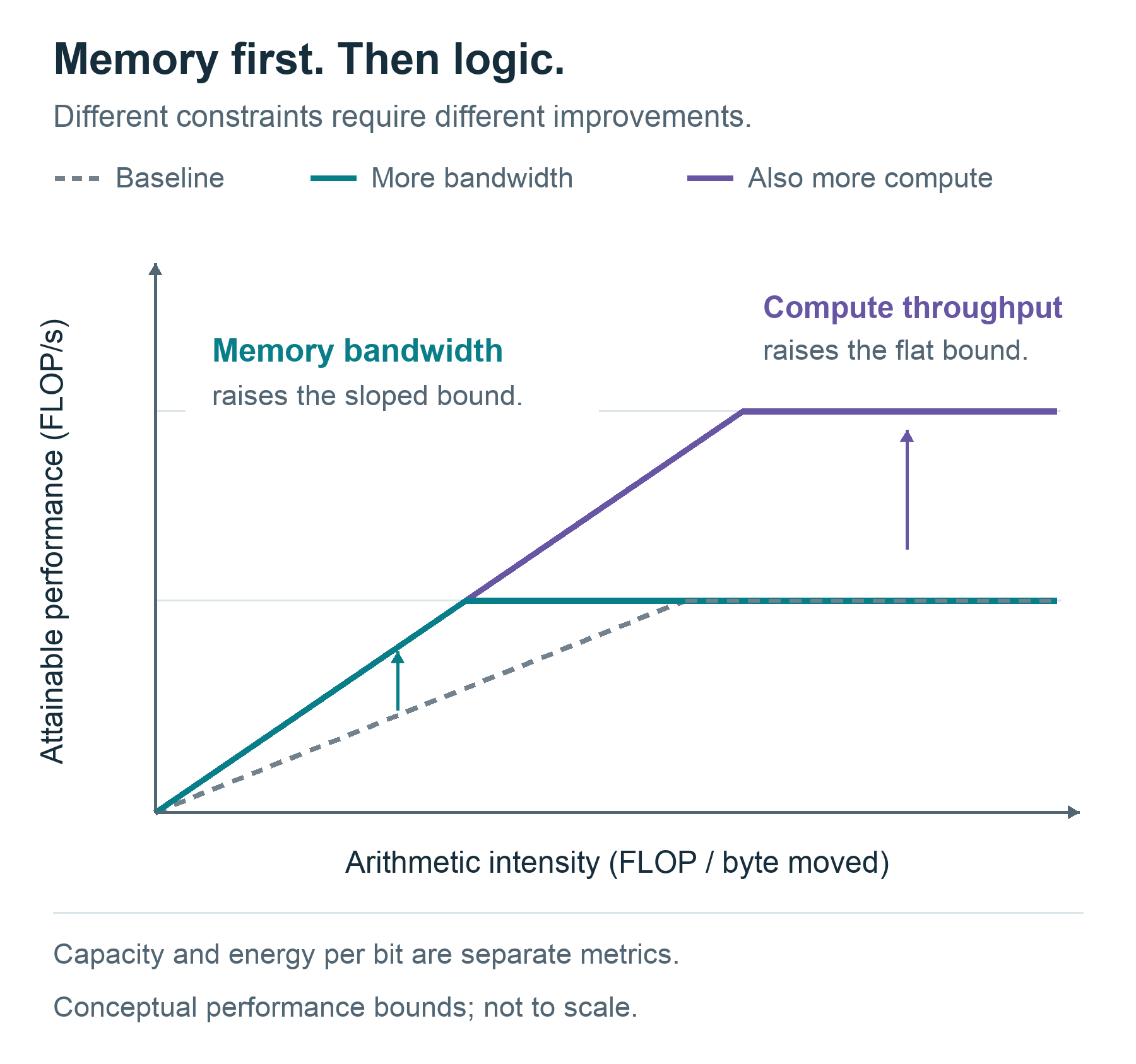
Figure 1: Start with memory and push to logic: Kepler technology addresses the core physical limits for TPS/W and interactivity (TPS/S/user) via Kepler memories that HBM and SRAM tier memories that push the pareto frontier on bandwidth per watt and capacity based on 3D and materials innovations. The Kepler logic roadmap pushes the logic bound workloads. All technologies are fully backward compatible and boost existing fabs/designs to higher Wafers/$ and TOPS/W.
The Kepler Master Plan: Memory first, logic next.
Memory is the harbinger of logic. In the 1980s, SRAM memory helped build confidence in the CMOS process11 which enabled the logic revolution12. Firmly rooted in the VLSI industries’ meticulous pathfinding process, we have extracted the master plan down to two steps:
ACT1: Address the memory and interconnect wall boosting memory capacity, memory bandwidth and memory E/bit. This involves developing both HBM and SRAM significantly beyond the roadmap.
ACT-1 Total Memory Capacity = Chips/Package X Memory efficiency/die X bit-cells/area. Total Memory Bandwidth = Interconnects/Package X Bits/package/s
Total Memory E/bit= Length X Capacitance/Length X V2
ACT2: New logic technology to lower cost and reduce the interconnect operating voltage below CMOS. We have made progress on logic densification, which we will present at an upcoming industry technical conference13. Our team has also invented multiple beyond-CMOS device candidates, including MESO14, developed while at Intel. We are excited to marry next generation transistor replacement devices invented at Kepler with AI-accelerated materials development15.
ACT-2 Total Logic Circuit Energy = Devices/Function X Charge X V Total Logic Function Density = Function/Device X Devices/area
Kepler drives the highest leverage factors to their physics limits.
Kepler’s Moore’s Law Economics: Kepler aims to unlock fab capacity and drop the time, cost and complexity of leapfrogging EUV-CMOS nodes by 10X. When our technology is applied to lagging nodes, they produce ~ 3 node acceleration and when applied to leading nodes, they produce equivalent densities beyond the EUV-CMOS roadmap.
Logic and SRAM Targets
| Before | 28 nm | 12 nm | 7 nm | 5 nm | 3 nm | 2 nm | 14A | 10A |
| After Kepler Upgrade | 7 nm | 3 nm | 2 nm | 2X 2 nm | >5A | >3A | >1A |
We apply the underlying philosophy of removing the EUV dependency for scaling to HBM class memories as well - enabling the leapfrogging of leading node DRAM-HBM systems.
Our technology is digital, room temperature, backwards compatible and agnostic to architecture and software. We do this without changing the digital abstraction layer, software, GPU/CPU/ASIC/FPGA architectures. We expect that the digital abstraction layer running at room temperature in billions of devices and thousands of datacenters today will continue to power a large fraction of the global economy. Kepler’s technology works at room temperature with inexpensive tooling and is perfectly compatible with mainstream computing’s hard earned software and algorithmic stack.
Kepler An American Story built with Global Partners: We are an American Startup rooted in the American way of problem solving. When America was challenged in the space race, America made one of the world’s first integrated-circuit computers—a machine that helped guide Apollo 11 to the lunar surface. Our rivals did not have the chips and we did. Chips are not an exception to the American story. From uranium enrichment and advanced steels to polymers and semiconductors, America has repeatedly won consequential races through innovation in materials. This is a uniquely American tradition: confronting enormous challenges with physics—and building what the world once thought impossible.
American invention is strengthened by trusted partners around the world. After the peace treaty, Benjamin Franklin wrote, “We are now Friends with England and with all Mankind.” Lee Kuan Yew urged policies that would cultivate “the largest number of reliable and strong friends.” Intelligence abundance will not be built by one company but by partners united by common ambition and values. Kepler is built in the image of that same spirit of cooperation.
We are working toward better HBM and SRAM for processor designers and more capital-efficient scaling for foundries. We are also discovering the next transistor that will drive the technology for decades to come. This effort depends on customers, tool makers, packaging and metrology partners, industrial engineers, public institutions and academic researchers. Above all, it depends on the people doing the work and the families who have supported them day and night. We thank you all !
Launch Day As astronaut Chris Hadfield observed on his launch day, while everyone else was driving away from the rocket loaded with explosive fuel, the astronauts kept moving toward it—not because they were blind to the danger, but because they had studied it, prepared for it, and learned to master it.
We know this is a hard problem. Many warned us that it was impossible. But we studied it, toiled in silence, and trained for this moment.
Now, we confronted its hardest challenges head-on—building toward a future of intelligence abundance.
We are open for business.
If you are designing an AI system constrained by memory capacity, memory bandwidth or latency, data delivery or power, we want to work with you on the right memory and integration approach. If you build the tools, precursors, devices or factories that can advance this mission, join us.
Kepler’s fabs and chips are steps toward compute and intelligence abundance—unleashing all of the human creativity currently trapped behind scarcity.
Join us— dreamers, prospectors, settlers, makers, partners, engineers, and builders—and help us create an abundance of intelligence.
Notes
- 1
Wu, S.Y., Chang, C.H., Chiang, M.C., Lin, C.Y., Liaw, J.J., Cheng, J.Y., Yeh, J.Y., Chen, H.F., Chang, S.Y., Lai, K.T. and Liang, M.S., 2022, December. A 3nm CMOS FinFlex™ platform technology with enhanced power efficiency and performance for mobile SoC and high performance computing applications. In 2022 International Electron Devices Meeting (IEDM) (pp. 27-5). IEEE.
↩ - 2
R. P. Colwell, “The Chip Design Game at the End of Moore’s Law,” 2013 IEEE Hot Chips 25 Symposium, pp. 1–16, 2013.
↩ - 3
Kuhn, K.J., Avci, U., Cappellani, A., Giles, M.D., Haverty, M., Kim, S., Kotlyar, R., Manipatruni, S., Nikonov, D., Pawashe, C. and Radosavljevic, M., 2012, December. The ultimate CMOS device and beyond. In 2012 International Electron Devices Meeting (pp. 8-1). IEEE.
↩ - 4
Micron, Fiscal Q2 2024 earnings presentation, slide 8: HBM3E requires approximately three times the wafer supply per bit of same-node DDR5. For a component-level memory-energy breakdown, see O’Connor et al., Fine-Grained DRAM: Energy-Efficient DRAM for Extreme Bandwidth Systems, MICRO 2017, Table 3. Capacitance depends on geometry and dielectric; link-switching energy is only part of total memory-access energy.
↩ - 5
A. Gholami, Z. Yao, S. Kim, C. Hooper, M. W. Mahoney, and K. Keutzer, “AI and Memory Wall,” IEEE Micro, 2024. See especially Figs. 1–2 and the accompanying discussion. Paper
↩ - 6
Cao, W., Bu, H., Vinet, M., Cao, M., Takagi, S., Hwang, S., Ghani, T. and Banerjee, K., 2023. The future transistors. Nature, 620(7974), pp.501-515.
↩ - 7
Bennett, C.H. and Landauer, R., 1985. The fundamental physical limits of computation. Scientific American, 253(1), pp.48-57.
↩ - 8
Manipatruni, S., Nikonov, D. E. & Young, I. A. Beyond CMOS computing with spin and polarization. Nature Physics 14, 338–343 (2018).
↩ - 9
Nikonov, D.E. and Young, I.A., 2013. Overview of beyond-CMOS devices and a uniform methodology for their benchmarking. Proceedings of the IEEE, 101(12), pp.2498-2533.
↩ - 10
Adhinarayanan, V. et al. Folded banks: 3d-stacked hbm design for finegrained random-access bandwidth. Proceedings of the 52nd Annual International Symposium on Computer Architecture 1819–1833 (2025)
↩ - 11
C. Webb, R. Creek, W. Holt, G. King, and I. Young, “A 65 ns CMOS 1Mb DRAM,” presented at the 1986 IEEE International Solid-State Circuits Conference (ISSCC), Session 19.2
↩ - 12
Moore, G.E., 1996. Intel: Memories and the microprocessor. Daedalus, 125(2), pp.55-80.
↩ - 13
Conference in December 2026
↩ - 14
Manipatruni, S., Nikonov, D.E., Lin, C.C., Gosavi, T.A., Liu, H., Prasad, B., Huang, Y.L., Bonturim, E., Ramesh, R. and Young, I.A., 2019. Scalable energy-efficient magnetoelectric spin–orbit logic. Nature, 565(7737), pp.35–42.
↩ - 15
Kepler was selected as part of the DOE Genesis Mission to further this work
↩